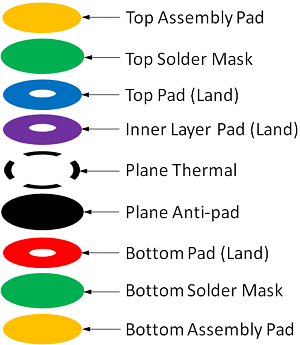
The SMT Padstack is easy -
- Top Land
- Top Solder Mask
- Top Paste Mask
- Top Assembly
Part 7 of this blog explains the Land Calculation for SMT land patterns, so let’s discuss Plated Through-hole calculations in this segment.
The Through-hole (PTH) Padstack is complex -
- Drill Hole
- Top Assembly
- Top Solder Mask
- Top Land
- Inner Land
- Plane Thermal Relief
- Plane Anti-pad (Clearance)
- Bottom Land
- Bottom Solder Mask
- Bottom Assembly
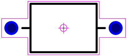
Here is a picture of a through-hole padstack.
PTH Padstack
The PTH padstack creation can be fully automated via the maximum lead diameter.
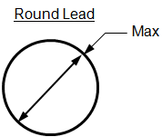
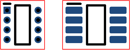
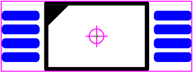
Round PTH Lead Rectangle PTH Lead
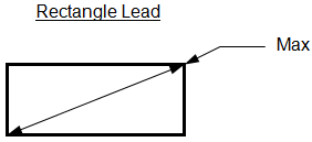
Rectangle PTH Lead
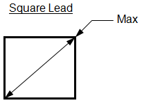
Square PTH Lead
In the IPC-2222 standard there is a hole size calculation chart -
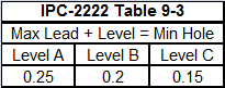
IPC-2222 Table 9-3
Once you calculate the hole size, the minimum annular ring is 0.05 mm.
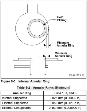
IPC-2221 Minimum Annular Ring
Next we need to add the IPC-2221 Minimum Fabrication Allowance to the pad size.
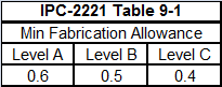
IPC-2221 Table 9-1
So the Minimum Annular Ring X 2 + Minimum Fabrication Allowance + Maximum Lead + Hole Over Lead = Pad Diameter
Next we need to calculate the Plane Thermal Relief ID, OD and Spoke Width sizes.
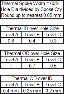
Thermal Relief Calculations
The Plane Anti-pad or Plane Clearance is the same size as the Thermal Relief OD (Outside Diameter).
In both the SMT and PTH padstack, the IPC recommended Solder Mask and Paste Mask size is 1:1 scale of the Top and Bottom land size. The PCB fabrication shop can automatically oversize (swell) the solder mask to any size they need to insure high yield production per their specific manufacturing capabilities. This is where automation of padstack generation comes in. The entire concept is to generate a padstack that meets the environment class of your design specification.
The IPC-7251 Through-hole land patterns have the capability of accommodating all three performance classifications.
Producibility Levels: When appropriate this standard will provide three design producibility levels of features, tolerances, measurements, assembly, testing of completion or verification of the manufacturing process that reflect progressive increases in sophistication of tooling, materials or processing and, therefore progressive increases in fabrication cost. These levels are:
- Level A General Design Producibility – Preferred [Maximum land\lead to hole relationship]
- Level B Moderate Design Producibility – Standard [Nominal land\lead to hole relationship]
- Level C High Design Producibility – Reduced [Least land\lead to hole relationship]
The producibility levels are not to be interpreted as a design requirement, but a method of communicating the degree of difficulty of a feature between design and fabrication/assembly facilities. The use of one level for a specific feature does not mean that other features must be of the same level. Selection should always be based on the minimum need, while recognizing that the precision, performance, conductive pattern density, equipment, assembly and testing requirements determine the design producibility level. The numbers listed within the tables of IPC-7251 are to be used as a guide in determining what the level of producibility will be for any feature. The specific requirement for any feature that must be controlled on the end item shall be specified on the master drawing of the printed board or the printed board assembly drawing.
Download the IPC-7251 padstack charts here - AppNote 10835: IPC-7251 Padstack Charts
Density Level A: Maximum Land/Lead to Hole Relationship – The ‘maximum’ land pattern conditions have been developed to accommodate the most robust producability of the solder application method. The geometry furnished may provide a wider process window for solder processing. The level A land patterns are usually associated with low component density product applications.
Density Level B: Nominal Land/Lead to Hole Relationship – Products with a moderate level of component density may consider adapting the ‘median’ land pattern geometry. The median land patterns furnished for all device families will provide a robust solder attachment condition for most soldering processes and should provide a condition suitable for wave, dip, drag or reflow soldering.
Density Level C: Least Land/Lead to Hole Relationship – High component density typical of portable and hand-held product applications may consider the ‘minimum’ land pattern geometry variation. Selection of the minimum land pattern geometry may not be suitable for all product use categories.
The “Proportional” PTH Padstacks are a mixture combination of all the IPC Levels. Small holes use Level C and medium hole sizes use Level B and large hole sizes use Level A. When a hole size exceeds 2 mm, the Proportional padstack annular ring will incrementally grow with every hole size. I have used the proportional padstacks for the past 20 years and it is proven technology that works. Its flexible flow is more compliant with the PTH components and their pin pitch density. The main point is that Proportional padstacks meet or exceed the IPC-7251 standard.
Download the Proportional padstack chart here - Appnote 10836: Proportional Through-hole Padstacks
Note: the “Producibility Levels” are not necessarily related to the IPC Preformance Classifications. i.e.: The IPC-7251 land patterns have the capability of accommodating all three performance classifications.
IPC Performance Classifications: Three general end-product classes have been established to reflect progressive increases in sophistication, functional performance requirements and testing/inspection frequency. It should be recognized that there may be an overlap of equipment between classes.
The end product user has the responsibility for determining the ‘‘Use Category’’ or ‘‘Class’’ to which the product belongs. The contract between user and supplier shall specify the ‘‘Class’’ required and indicate any exceptions or additional requirements to the parameters, where appropriate.
Class 1 General Electronic Products – Includes consumer products, some computer and computer peripherals, and hardware suitable for applications where the major requirement is function of the completed assembly.
Class 2 Dedicated Service Electronic – Products Includes communications equipment, sophisticated business machines, and instruments where high performance and extended life is required, and for which uninterrupted service is desired but not mandatory. Typically the end-use environment would not cause failures.
Class 3 High Reliability Electronic Products – Includes all equipment where continued performance or performance-on-demand is mandatory. Equipment downtime cannot be tolerated, end-use environment may be uncommonly harsh, and the equipment must function when required, such as life support systems and other critical systems.