The IPC-7351B standard only focuses on 2 two major aspects of the CAD library:
- The land size and spacing
- Placement courtyard
All of the other aspects of the CAD library part such as silkscreen & assembly outlines, polarity markings, ref des, centroid marking, etc. are considered user definable drafting items. This includes all of the rules that pertain to these items such as line widths, silkscreen to land spacing, polarity sizes, ref des height, etc. are not part of the standard. But the Placement Courtyard Boundary is defined in the IPC-7351B standard, but the line width used to create the outline is user definable. The default solder mask and paste mask values are mentioned in the IPC-7351 as to be 1:1 scale of the land size, but this is only a recommendation.
See Courtyard Determination pictures below to see the 3 outlines defined by IPC-7351 as:
- Maximum Component Boundary
- Minimum Placement Courtyard
- Courtyard Manufacturing Zone

Surface Mount Courtyard Determination

Plated Through-hole Courtyard Determination
Here are the standard spacing rules from the Maximum Component Boundary to the Minimum Placement Courtyard:
- Least Environment = 0.1 mm
- Nominal Environment = 0.25 mm
- Most Environment = 0.5 mm
There are different Placement Courtyard spacing rules for Grid Array packages based on ball size:
- Ball size above 0.50 mm = 2 mm
- Ball size between 0.50 mm & 0.25 mm = 1 mm
- Ball size below 0.25 mm = 0.5 mm
One of the key aspects of the placement courtyard is that it allows room for rework. In the case of the BGA’s, the larger the Ball Size, the larger the heat nozzles and removal equipment is for getting around and under the component to unsolder the contacts. An important note to make here is that if you have no intentions of ever reworking (remove and replace) a BGA component then the 2 mm placement courtyard is not necessary and a 0.5 mm courtyard excess is OK. This also is relevant to the “Most Environment” where the minimum courtyard excess is 0.5 mm on all SMT land patterns. i.e.: the military and medical instrument industry might use the Most Environment and require “Class 3″ High Reliability Electronic Products where continued high performance is critical and product downtime cannot be tolerated. The “Class 3″ fabrication is very expensive and if a component on the PCB fails, rework becomes necessary to reduce cost. Rework requires additional land pattern placement courtyard excess to allow adequate space for rework equipment. Alternatively, the “Least Environment” for High Density PCB Layout, like handheld devices, has a courtyard excess of 0.1 mm with no room for rework equipment. So if a component fails in your Cellular Phone it will not be sent back to the shop for rework, but instead, it will be discarded.
The Placement Courtyards can be placed next to each other so the outline overlaps, however you need to discuss this with your assembly shop if they require an additional Manufacturing Zone for their process. The Placement Courtyard round-off snap grid is 0.5 mm. The question of “why don’t you place the silkscreen outline outside the land pattern boundary” is a FAQ and this is the answer - ”It is important that all silkscreen outline data be located inside the Placement Courtyard”.
This includes the Post Assembly Inspection Dot, which sometimes gets partially placed outside the placement courtyard. This is why in the upcoming IPC-2614 for Board Fabrication Documentation and drafting standards the “Post Assembly Inspection Dot” will become the “Post Assembly Inspection Line” and it will look like this to keep them inside the Placement Courtyard:
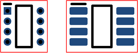
DIP & SOP Post Assembly Inspection Line
The Placement Courtyard or Courtyard Excess is the smallest area that provides a minimum electrical and mechanical clearance of the maximum extremities of the land pattern and/or the component body. However it is the responsibility of the user to verify the land patterns used for achieving an undisturbed mounting process including testing and an ensured reliability for the product stress conditions in use.
For many through-hole parts and connectors, the placement courtyard will follow the contour of the component body outline and land pattern.
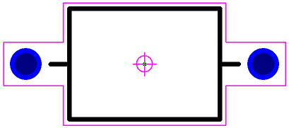
Axial Lead Courtyard
Most Enterprise CAD tools like Mentor Expedition have a different DRC checking feature that the user can define the component type to component type spacing rules. In this case, the placement courtyard excess should be turned off and the placement courtyard would be identical to the Maximum Component Boundary.
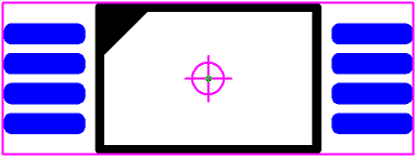
Enterprise CAD Tool Courtyard
The Enterprise CAD tool placement courtyard is not defined in the IPC-7351 standard. This concept is based on the Enterprise CAD tools ability to determine various component body to body spacing that is user definable.
No comments:
Post a Comment